56th,IBM announces the creation of the world's first 2nm semiconductor chip。IBM said,under the same power consumption,245% higher performance than current 7nm EUV chips,Output the same performance but reduce power consumption by 75%。
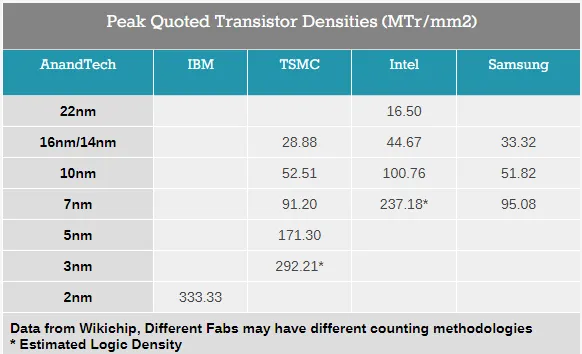
Core indicators,IBM claims the transistor density of the 2nm chip (MTr/mm2,How many million transistors per square millimeter) is 333.33,Almost twice as much as TSMC's 5nm,It is also higher than the TSMC 3nm process 292.21 MTr/mm2。
In other words,Within 150 square millimeters, the size of the fingernail,Can accommodate 50 billion transistors。Simultaneously,IBM said,Under the same power consumption,Its performance is 45% higher than the current 7nm,The output performance reduces power consumption by 75%。
Actually,IBM was the first manufacturer to build 7nm (2015) and 5nm (2017) chips.,The decision of voltage and other indicators has long been taken to take the dominance of the power。
Back to this 2nm,GAA (surround gate transistor) technology is used,Three layers。Introduction to IBM,This is the first time that the bottom dielectric isolation channel is used,It can achieve a gate length of 12 nm,Its internal spacing is the second generation dry method design,Helps in the development of nanosheets。This is also the first time using EUV to expose part of FEOL。
have to be aware of is,IBM does not have its own wafer fab,2014In 2019, its manufacturing factory was sold to GS,But the two signed a 10-year cooperation agreement,in addition,IBM and Samsung、Intel keeps collaborative。
About GAA transistor technology,Samsung 3nm、Intel 5nm and TSMC 2nm will be used for the first time。
source:IBM